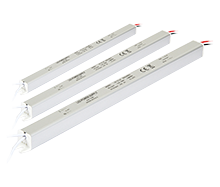
What are the specific processes for the circuit board of LED switch power supply?
There are many surface treatment processes for PCB circuit boards of switch power supplies, including hot air leveling, organic coating, chemical nickel plating/immersion gold, silver deposition, tin deposition, etc. Now let's introduce it to us in detail.
1. Hot air leveling
Hot air leveling, also known as tin spraying, is a commonly used processing technique for PCB boards in early switch power supplies. It involves coating the PCB with molten tin lead solder and leveling it with heated compressed air to form a coating layer that is both resistant to copper oxidation and provides excellent solderability.
2. Organic coating
This process is different from other surface treatment processes, as it serves as a barrier layer between copper and air; Simply put, this process involves chemically growing an organic film on a clean bare copper surface. This layer of film has oxidation resistance, heat shock resistance, and moisture resistance, mainly used to protect the copper surface from further rusting in normal environments; It is also necessary to be easily removed by the soldering flux during the subsequent welding process at high temperatures, in order to facilitate welding. The organic coating process is simple and cost-effective, and is widely used in the manufacturing of circuit boards for switch power supplies.
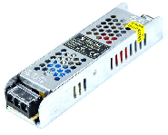
3. Chemical nickel plating/immersion gold
Chemical nickel plating/immersion gold is not as simple as organic coating technology, requiring a thick layer to be wrapped around the copper surface. Unlike organic coating, which only serves as a rust proof barrier layer, the nickel gold alloy with excellent electrical function can protect the PCB of the switching power supply for a long time and achieve outstanding electrical function. It also has environmental resistance that other surface treatment processes do not possess, effectively preventing damage to the PCB board.
4. Sinking Silver
The silver deposition process is relatively simple and fast, and is between organic coating and electroless nickel plating/immersion gold. Silver deposition does not require a thick layer of armor to be applied to the PCB board of the switch power supply. It can provide good electrical function and maintain excellent solderability to the PCB board in hot, humid, and polluted environments. The defect is that it will lose its luster. Other types of sunk silver also have outstanding storage properties, and generally can be assembled after several years without major problems.
5. Sinking tin
Because all current solder materials are based on tin, the tin layer can match any type of solder, which also makes the tin deposition process have good development prospects. In the past, when the tin deposition process was not perfect, the PCB board of the switching power supply was prone to tin whiskers after tin deposition, which caused reliability issues during the soldering process due to tin whiskers and tin migration. Nowadays, organic additives have been added to the tin deposition solution to give the tin layer a granular structure, overcoming the problem of tin whiskers. It also has good thermal stability and weldability, enhancing its applicability.
What are the common PCB surface processes for switch power supplies? Let's first introduce them. There are other types of surface processes for PCB circuit boards, such as nickel gold plating, nickel palladium plating, etc., which are more difficult to manufacture and costly than the aforementioned processes, so they have not been widely used.
Article source: Jiangmen LED Switching Power Supply http://www.gddpdz.com/
-
01-08
The lighting exhibition has successfully concluded, with abundant harvest!
Dubai International Smart Lighting ExhibitionJanuary 14-16, 2025
-
01-08
Notice of Spring Festival holiday in 2025
Dear customer:Please be informed that our company's Spring Festival holiday is scheduled from January 18, 2025 to February 12, 2025, during which business will be temporarily suspendedStarting fr
-
10-28
Jiangmen LED Switching Power Supply: Protection Methods for LED Driver Power Circuit
Using a fuse (tube) to protect the LED circuitBecause fuses are disposable and have slow response times, poor effectiveness, and are difficult to use, fuses are not suitable for LED light products, as
-
10-21
Advantages and Characteristics of Jiangmen Waterproof Power Supply Manufacturer's Products
LED waterproof power products are designed with integrated components, featuring low temperature rise, low heat generation, power output voltage limit and constant current. High quality device coopera

